

Model: VM-X3S
VM-X3S Small size reader module specifications

-Based on the new generation Impinj E310 reader chip.
-Supports EPC global UHF Class 1 Gen2 (ISO 18000-6C).
-27dBm RF output.
-The SMD form is convenient for rapid packaging production.
-Real-time temperature monitoring.
-It has low power consumption , is only the size of a coin, and can be easily integrated into different types of RFID devices, such as proximity reading and writing devices or portable Bluetooth printers.
FEATURES
SPECIFICATIONS
Model No | VM-X3S |
Physical parameters | |
2 1 mm L x 2 1 mm W x 3. 7 mm H | |
weight | 2.8 g |
RF parameters | |
Air interface protocol | EPC global UHF Class 1 Gen 2 (ISO 18000-6C) |
chip | Impinj E310 |
frequency | North America: 902-928MHz FCC (NA, SA) |
Europe: 865-868MHz (ETSI) | |
China: 920-925MHz (CMIIT) | |
Full frequency band: 860-960MHz (OPENˊ) | |
Antenna connection | 1 RF interface (bottom pad) |
power | 5dBm- 27dBm (±1dB) adjustable |
Sensitivity | -73dBm@10%BER |
Working Mode | Fixed frequency/hopping frequency optional |
RSSI | support |
interface | |
Support API | C, C#/.NET, Java |
RF Performance | |
Label inventory peak speed | >300 tags/s |
Reading distance | >3 meters (using 2.5dBi ceramic antenna) |
Tag Buffer | 1000 labels @96 bit EPC |
Communication interface | |
Communications | 20-pin stamp hole communication (SMT compatible) Baud rate 9600~921600bps@Default 115200bps |
GPIO (optional) | 2 inputs and 2 outputs (3.3V TTL) |
communication | SMD Uart3.3V (TTL) |
powered by | |
Voltage | DC 5V±5% |
Power consumption | 3.25W (peak), 0.65A@5V, 27dBm |
Standby power consumption | 0.75W |
Environmental parameters | |
Operating temperature | -20°C to +5 5 °C |
Storage temperature | -40°C - +85°C |
humidity | 5-95% non-condensing (+25°C) |
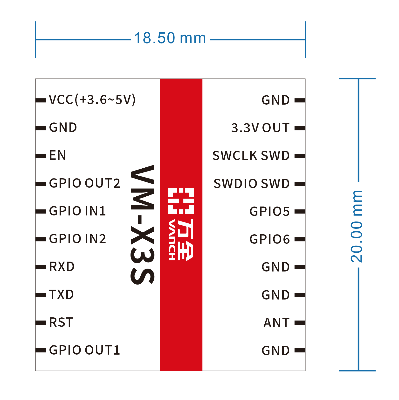
Pinout | definition | Pinout | definition |
1 | VCC (+3.6~5V) | 11 | GND |
2 | GND | 12 | 3.3V Output |
3 | EN module power enable LOW (POWER DOWN) HIGH & DISCONNECT (ACTIVE) |
13 | SWCLK SWD programming interface clock line |
4 | Digital Output 2 (GPIO OUT2) | 14 | SWDIO SWD burning interface data cable |
5 | Digital Input 1 (GPIO IN1) | 15 | GPIO5(RFU) |
6 | Digital Input 2 (GPIO IN2) | 16 | GPIO6 (RFU) |
7 | RXD (DATA INPUT, TTL level) | 17 | GND |
8 | TXD (DATA OUTPUT, TTL level) | 18 | GND |
9 | RST (LOW ACTIVE, leave it unconnected if not in use) | 19 | ANT |
10 | Digital Output 1 (GPIO OUT1) | 20 | GND |
PACKING LIST
DOWNLOAD
ENQUIRY
If you have any good suggestions and comments on our company, or want to consult our products, please fill in the form below, and we will contact you at the first time!
RELATED PRODUCTS

Products
Contact us
Shenzhen Vanch Intelligent Technology Co.,Ltd
Tel: +86 0755-82426775
Email: sales@vanch.net
ADD: 3rd Floor, Fuding Industrial Park, No. 17 Tianxi Road, Fucheng Street, Longhua District, Shenzhen city- 518110, Guangdong Province, China
American Branch
Tel: +1-949 878 1689
Email: steven_reputa@163.com
Contact person: Mr. Zhang
ADD: 7 Scouting Blvd, Medford, NY11763
Copyright © 2026 Shenzhen Vanch Intelligent Technology Co., Ltd.